Welcome to DU!
The truly grassroots left-of-center political community where regular people, not algorithms, drive the discussions and set the standards.
Join the community:
Create a free account
Support DU (and get rid of ads!):
Become a Star Member
Latest Breaking News
Editorials & Other Articles
General Discussion
The DU Lounge
All Forums
Issue Forums
Culture Forums
Alliance Forums
Region Forums
Support Forums
Help & Search
Science
Related: About this forumA Scientific Theater of the Absurd: Solar CVD of Graphene.
I came across this paper this evening and don't know whether to laugh or cry:
High-Quality AB Bilayer Graphene Films by Direct Solar-Thermal Chemical Vapor Deposition Abdalla Alghfeli and Timothy S. Fisher, ACS Sustainable Chemistry & Engineering 2023 11 (32), 11719-11728
The paper starts off serious enough:
Graphene consists of carbon atoms arranged in a two-dimensional honeycomb lattice structure (1) whose thickness varies between one and a few stacked layers. Its exceptional properties include high thermal and electrical conductivities, (1,2) optical transmissivity, (3) excellent chemical stability, (4) and high mechanical flexibility (5) and strength. (6) Consequently, graphene has been studied in many energy conversion and storage applications such as flexible solar cells, (5,7) sunlight-activated transparent electrodes, (4) supercapacitors, (8−10) lithium-ion batteries (10,11) and water-splitting processes. (10) In addition, Bernal-stacked (“AB”) bilayer graphene has a tunable bandgap by an external electric field that can be employed for transistor applications. (12,13) Graphite exfoliation techniques by liquid-phase (14) and shear-mixing (15) processes can potentially scale up graphene production for industrial needs. For example, graphene production by exfoliation using tannic acid in an aqueous medium has been developed with an efficient methodology. (14) However, chemical vapor deposition (CVD) remains the most efficient method for mass production by employing roll-to-roll processing. (16,17) CVD allows some control of both graphene quality and thickness through growth kinetics and thermodynamics. (18−23)
Many prior studies have used plasma CVD to synthesize single-layer graphene (SLG) as transparent conducting electrodes with uniform sheet resistance and optical transmittance, (17) as well as freestanding graphene layers. (24) Others have focused on manufacturing supercapacitors and electrode materials such as bioinspired microconduits (8) and polygonal carbon nanofibers (9) that exhibit high areal capacitance, cyclic stability, and rate capability...
Many prior studies have used plasma CVD to synthesize single-layer graphene (SLG) as transparent conducting electrodes with uniform sheet resistance and optical transmittance, (17) as well as freestanding graphene layers. (24) Others have focused on manufacturing supercapacitors and electrode materials such as bioinspired microconduits (8) and polygonal carbon nanofibers (9) that exhibit high areal capacitance, cyclic stability, and rate capability...
Then there's this note:
Despite graphene’s use in many sustainable energy applications, its synthesis process is ecologically and economically costly. Graphene synthesis, specifically by CVD, consumes high energy, whether using plasma or electric heating sources. Studies have shown that the semiconductor industry, generally, contributes up to 2% of the manufacturing sector’s electricity consumption in the US, (36) where such expenses contribute up to 40% of fabrication costs. (36,37) Additionally, large semiconductor fabrication plants consume up to 100 MWh of energy each hour, (37) where approximately 0.386 kg of carbon dioxide is released per kWh according to the U.S. Energy Information Administration in 2020. (38) In 2020, CVD technologies in the microelectronics industry were found to contribute up $14–15 billion to the US economy and were associated with up to 62% of total market revenues. (39) Nevertheless, electrical energy consumption and CO2 emissions for 300 mm wafer fabrication were estimated to be 1400 kWh/wafer and 300 kg/wafer, (39) respectively, and continue to increase with new technologies to achieve smaller Moore’s law nodes...
The solution?
In the present work, we demonstrate the use of direct solar capture to synthesize high-quality AB-stacked graphene films with up to 91% coverage in a fast one-step process. Prior studies have reported AB-bilayer graphene growth on polycrystalline copper through a two-step process (12) by synthesizing a top AB layer on a previously grown single layer, where at least 30 min growth time is required to achieve 30–67% AB coverage. Others have adopted low-pressure nucleation and high-pressure growth steps to achieve coverage up to 90% in 3 h. (13) Single-crystal Cu(111) (21) and Cu/Ni(111) alloy foils (46) enable the synthesis of high AB coverage of near 95% in a relatively short time between 2 and 20 min. However, this approach comes at the expense of using costly high-quality single-crystal copper or intricate sample preparation such as polishing and annealing over a 3–7 h period.
So we build manufacturing plants with all this apparatus, and we run the plants whenever the sun is shining. No night shift, and no one comes to work if its raining, cloudy or snowing, or the skies are filled with smoke from ecosystems because all our "solar energy will save us" fantasies have done zero to address climate change.
Stranger and stranger.
The apparatus we should build to operate a few hours a day on sunny days:
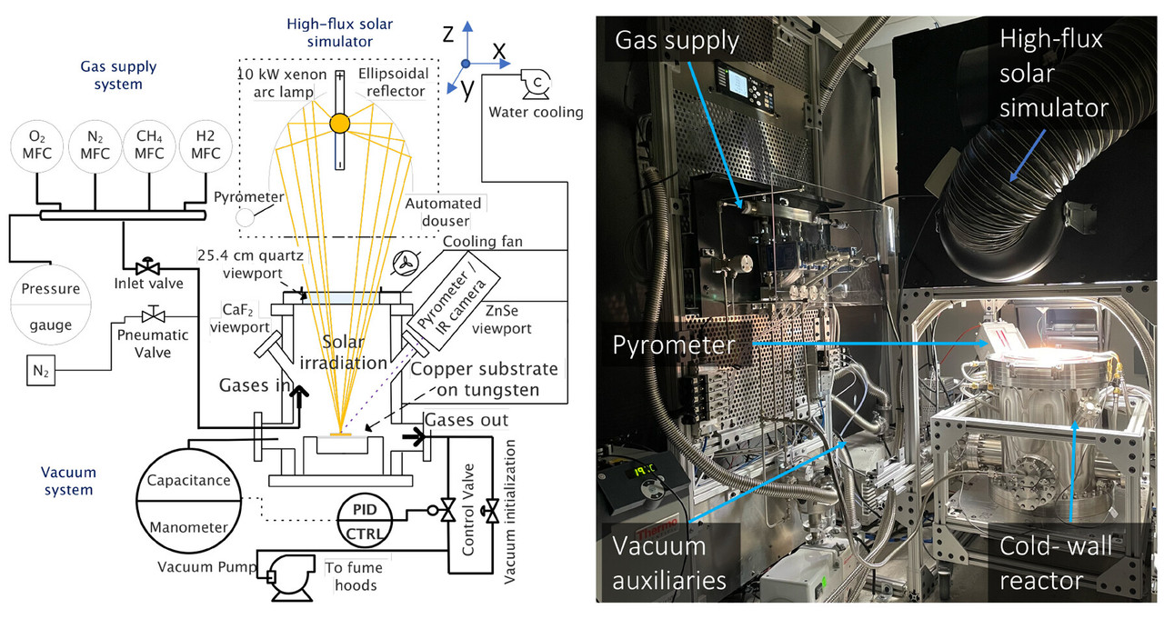
The caption:
Figure 1. Overview of the solar-thermal CVD setup for graphene synthesis.
The amusing thing is that to not have graduate students sitting around on the campus lawns waiting for the sun to shine, in other words to save time, they substituted a xenon lamp for the sun.
Anyway, once again, again and again and again and again, we're saved.
One sees this sort of thing, and one doesn't really want to believe it.
Sigh...
I trust you're enjoying your weekend.
1 replies
 = new reply since forum marked as read
Highlight:
NoneDon't highlight anything
5 newestHighlight 5 most recent replies
= new reply since forum marked as read
Highlight:
NoneDon't highlight anything
5 newestHighlight 5 most recent replies
= new reply since forum marked as read
Highlight:
NoneDon't highlight anything
5 newestHighlight 5 most recent replies
A Scientific Theater of the Absurd: Solar CVD of Graphene. (Original Post)
NNadir
Aug 2023
OP
usonian
(17,200 posts)1. Whatever happened to pencil smudges and Scotch tape?
Asking for a friend.